저차원 소재 및 소자 연구실(LDMD)
Low-Dimensional Materials & Devices Lab.
보유 장비
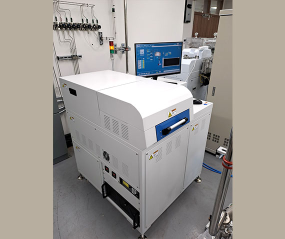
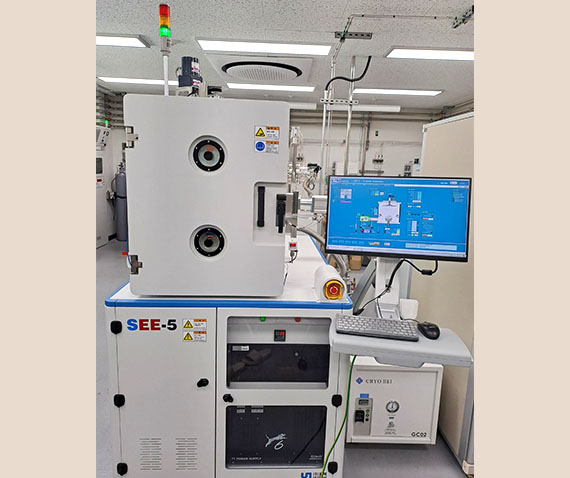
No. 1
Atomic Layer Deposition
설치위치
- Building 35 (Natural Sciences Hall 5)
장비스펙
- Supports deposition of Al2O3, HfO2
장비소개
- A system that precisely grows thin films at the atomic level using gaseous precursors
활용분야
- Fields that require high uniformity and precise control, such as semiconductor device fabrication and nanomaterial synthesis
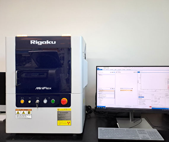
No. 2
X-Ray Diffractometer
설치위치
- Building 35 (Natural Sciences Hall 5)
장비스펙
장비소개
- An instrument that analyzes crystal structure, phases, and lattice constants by irradiating a material with X-rays and measuring the resulting diffraction pattern.
활용분야
- Fields involving the development of materials and the evaluation of quality across various applications such as semiconductors, batteries, ceramics, and other advanced materials
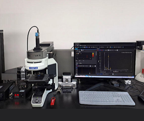
No. 3
Raman Spectroscopy
설치위치
- Building 35 (Natural Sciences Hall 5)
장비스펙
장비소개
- An instrument that analyzes molecular vibrations or lattice vibrations of a material using laser light.
활용분야
- Fields of materials engineering and life sciences.
- Used for analyzing chemical composition, crystallinity, stress, and defects of materials.
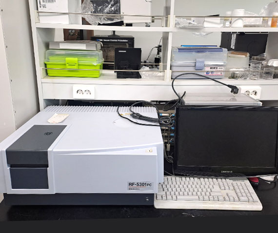
No. 4
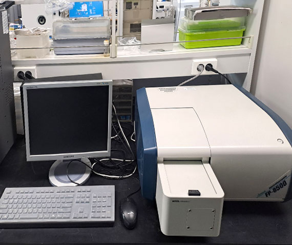
Spectrofluorophotometer
설치위치
- Building 35 (Natural Sciences Hall 5)
장비스펙
- Capable of measuring liquid samples.
장비소개
- An instrument that analyzes the light-emitting properties of a sample to evaluate its electronic characteristics.
활용분야
- Fields of semiconductor, nanomaterials, and optoelectronic device development.
No. 5
Spectrofluorophotometer
설치위치
- Building 35 (Natural Sciences Hall 5)
장비스펙
- Capable of measuring powders, liquid samples, and quantum dots.
장비소개
- An instrument that analyzes the light-emission properties of a sample to evaluate its electronic characteristics.
활용분야
- Fields of semiconductor, nanomaterial, and quantum dot research, as well as optoelectronic device development.
No. 6
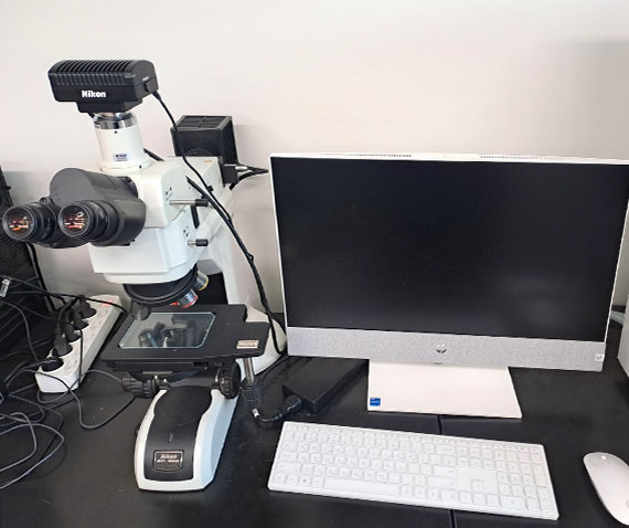
Optical Microscope
설치위치
- Building 35 (Natural Sciences Hall 5)
장비스펙
- Magnification range: 50× to 1000×
장비소개
- An instrument that magnifies and observes samples using visible light.
활용분야
- Fields of materials science and electronic devices.
- Visually analyzes microscopic structures such as material surfaces and micro-defects.
No. 7
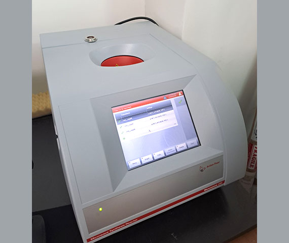
Microwave Reactor
설치위치
- Building 35 (Natural Sciences Hall 5)
장비스펙
- Maximum temperature: 230 °C, maximum pressure: 20 bar, capacity: up to 18 ml.
장비소개
- An instrument that uses microwaves to rapidly and uniformly heat samples, thereby accelerating chemical reactions.
활용분야
- Applications include new material synthesis, organic chemistry, and nanomaterial synthesis.
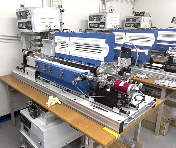
No. 8
Chemical Vapor Deposition
설치위치
- Building 35 (Natural Sciences Hall 5)
장비스펙
- Capable of conducting experiments under atmospheric pressure using gases such as H2, N2, and H2S.
장비소개
- An instrument that deposits thin films by thermally decomposing gaseous precursors.
활용분야
- Applications include semiconductors, displays, solar cells, and nanomaterial synthesis.
No. 9
E-beam evaporator
설치위치
- Building 35 (Natural Sciences Hall 5)
장비스펙
- Thickness and deposition rate can be controlled.
장비소개
- An instrument that forms thin films by evaporating materials such as metals or oxides at high temperatures using an electron beam.
활용분야
- Various precision thin-film deposition applications, including semiconductor device fabrication, optical coatings, sensor manufacturing, and nanotechnology research.
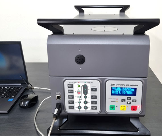
No. 10
Residual Gas Analyzer
설치위치
- Building 35 (Natural Sciences Hall 5)
장비스펙
장비소개
- An instrument that precisely detects and analyzes trace gases inside a vacuum chamber using mass spectrometry.
활용분야
- Used in materials research and vacuum equipment maintenance for applications such as contamination assessment of vacuum systems and monitoring of reactive gases.
No. 11
Metal Organic Chemical Vapor Deposition
설치위치
- Building 35 (Natural Sciences Hall 5)
장비스펙
장비소개
- An instrument that grows solid thin films using metal-organic compounds as precursors.
활용분야
- Used for high-quality thin film fabrication in applications such as LEDs, semiconductor devices, high-frequency components, and power devices.
No. 12
Sputtering
설치위치
- Building 35 (Natural Sciences Hall 5)
장비스펙
- Equipped with Mo, W, and Ni targets.
장비소개
- An instrument that uses plasma ions to bombard a target material, causing fine particles to sputter off and deposit as a thin film on a substrate.
활용분야
- Applications include semiconductors, displays, solar cells, and metal thin-film coatings.
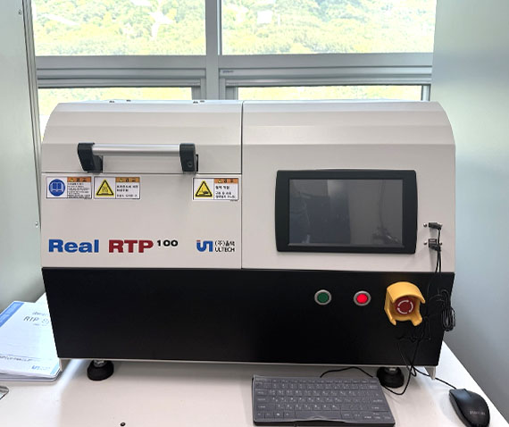
No. 13
Rapid Thermal Processing
설치위치
- Building 35 (Natural Sciences Hall 5)
장비스펙
장비소개
- A thermal processing instrument that rapidly heats or cools substrates.
활용분야
- Applications include semiconductor processes such as annealing and dopant activation, thin film crystallization, and junction formation.
No. 14
Plasma-Chemical Vapor Deposition
설치위치
- Building 35 (Natural Sciences Hall 5)
장비스펙
- Capable of using gases such as H2, N2, H2S, and CH4; pressure can be controlled via a throttle valve; plasma generation is possible.
장비소개
- A chemical vapor deposition (CVD) system that uses plasma to deposit thin films.
활용분야
- Applications include semiconductor thin film fabrication, displays, solar cells, sensors, and protective coatings.
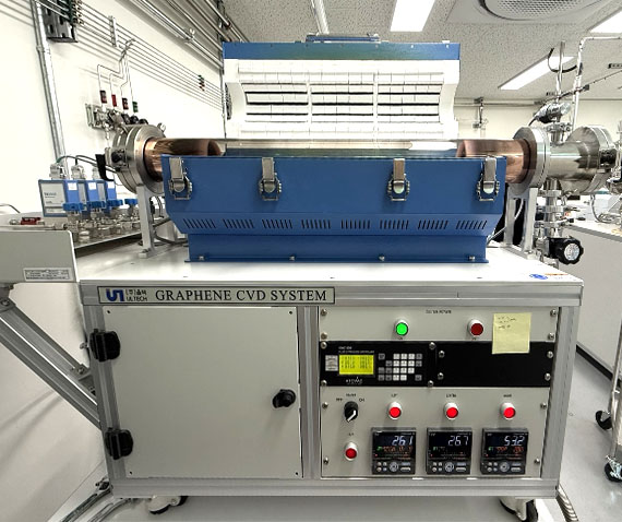
No. 15
Graphene-Chemical Vapor Deposition
설치위치
- Building 35 (Natural Sciences Hall 5)
장비스펙
장비소개
- An instrument that deposits thin films by using heat to decompose gaseous precursors.
활용분야
- Applications include graphene synthesis, thin film deposition, and thin film fabrication.
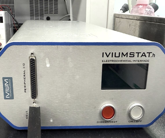
No. 16
Electrochemical Workstation
설치위치
- Building 35 (Natural Sciences Hall 5)
장비스펙
- Maximum current: ±5 A, maximum voltage: ±10 V, current accuracy: 0.6 aA, impedance base frequency range: 10 μHz to 8 MHz.
장비소개
- An electrochemical analysis instrument capable of performing various experiments such as LSV (Linear Sweep Voltammetry), CV (Cyclic Voltammetry), and EIS (Electrochemical Impedance Spectroscopy).
활용분야
- Electrochemical applications including water-splitting catalyst evaluation, battery research, sensor development, and corrosion studies.
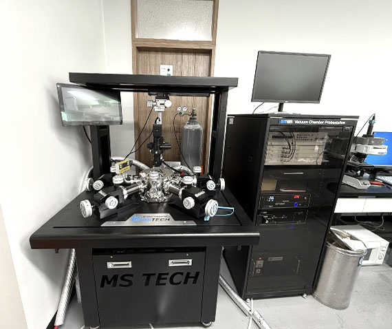
No. 17
Probe Station
설치위치
- Building 35 (Natural Sciences Hall 5)
장비스펙
- Temperature controllable.
장비소개
- An instrument that measures the electrical properties of semiconductor devices or materials using microprobes.
활용분야
- Applications include semiconductor device development, material property evaluation, and electrical reliability testing.
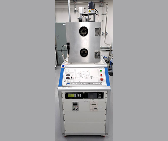
No. 18
Thermal Evaporator
설치위치
- Building 35 (Natural Sciences Hall 5)
장비스펙
- Capable of depositing various thin films depending on the deposition source.
장비소개
- An instrument that forms thin films on a substrate by vaporizing metals or organic materials using resistive heating.
활용분야
- Applications in thin-film device fabrication, including semiconductor electrodes, optical coatings, OLEDs, and solar cell manufacturing.