차세대반도체소자연구실(ASDL)
Advanced Semiconductor Device Laboratory
보유 장비
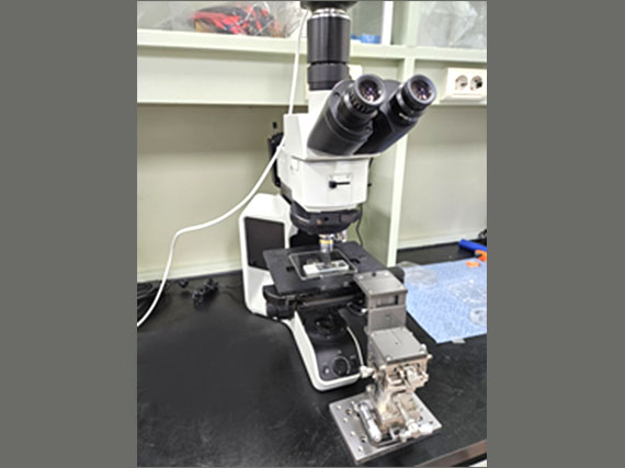
No. 1
Optical microscope
설치위치
- Room 104, Building 98 (Global Lifelong Learning Center)
장비스펙
- Magnification range: 100× to 1000×, bright field/dark field.
장비소개
- A microscope that visually magnifies micro-sized objects.
활용분야
- Optical imaging of 2D semiconductor electrons and semiconductor devices, etc.
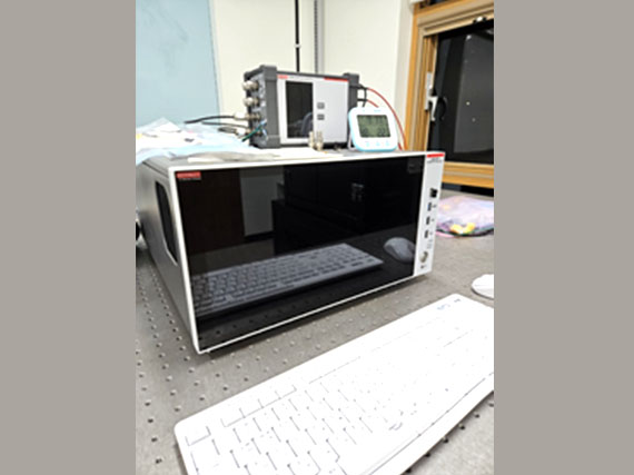
No. 2
Parameter analyzer
설치위치
- Room 104, Building 98 (Global Lifelong Learning Center)
장비스펙
- 10aA – 1A, 0.2µV – 210V, ±40V(80V p-p), ±800mA 200MSa/sec, 5ns 샘플링 레이트
장비소개
- Equipment for analyzing the electrical properties of semiconductor devices.
활용분야
- Measurement of I-V and C-V characteristics of semiconductor devices.
- Photocurrent measurement of optoelectronic devices.
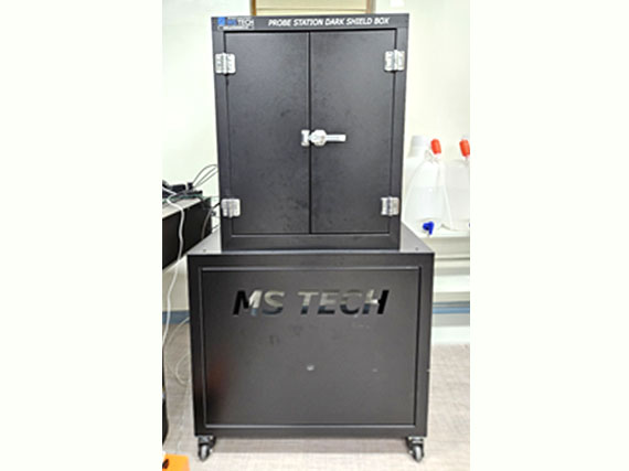
No. 3
MST5500B
설치위치
- Room 104, Building 98 (Global Lifelong Learning Center)
장비스펙
- 4 Micro positioner, dark shield box
장비소개
- Physical contact is established to measure the electrical properties of semiconductor devices.
활용분야
- Measurement of I-V and C-V characteristics of semiconductor devices.
- Photocurrent measurement of optoelectronic devices.
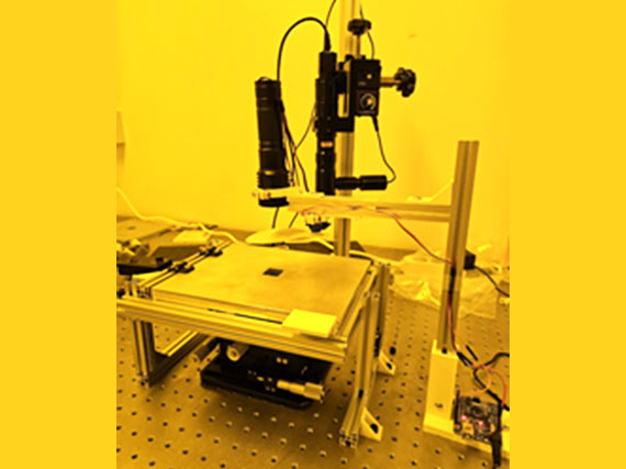
No. 4
Mask Aligner
설치위치
- Room 104, Building 98 (Global Lifelong Learning Center)
장비스펙
장비소개
- A mask alignment system for photolithography exposure.
활용분야