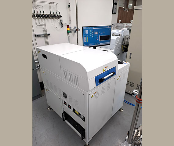
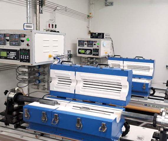
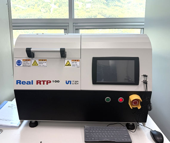
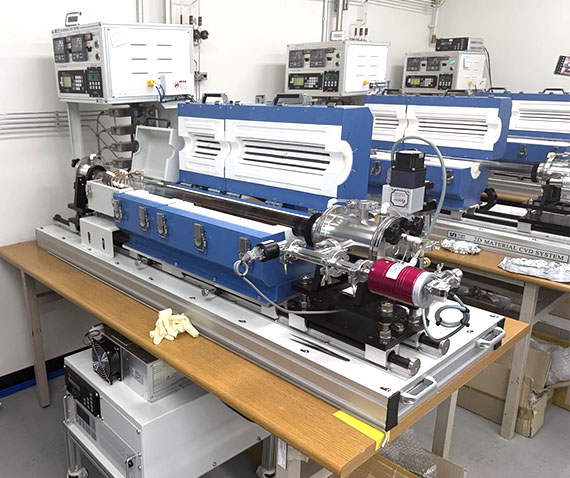
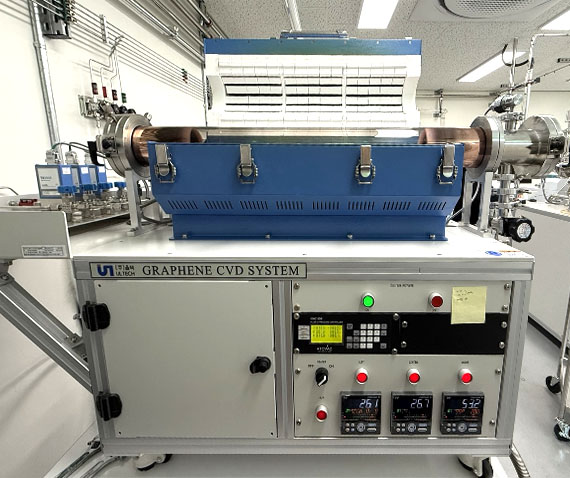
Low-Dimensional Materials & Devices Lab. > individual

본문 바로가기
사이트 내 전체검색

Individual Labs

HOME Facilities Individual Labs

Low-Dimensional Materials & Devices Lab.

Professor

  • Professor Jinsung Kwak

Available Equipment

장비 이미지
No. 1
Atomic Layer Deposition
Location
  • Building 35 (Natural Sciences Hall 5)
Specifications
  • Supports deposition of Al2O3, HfO2
Description
  • A system that precisely grows thin films at the atomic level using gaseous precursors
Applications
  • Fields that require high uniformity and precise control, such as semiconductor device fabrication and nanomaterial synthesis
장비 이미지
No. 2
X-Ray Diffractometer
Location
  • Building 35 (Natural Sciences Hall 5)
Specifications
  • 40kW, 15mA, 0.6kW
Description
  • An instrument that analyzes crystal structure, phases, and lattice constants by irradiating a material with X-rays and measuring the resulting diffraction pattern.
Applications
  • Fields involving the development of materials and the evaluation of quality across various applications such as semiconductors, batteries, ceramics, and other advanced materials
장비 이미지
No. 3
Raman Spectroscopy
Location
  • Building 35 (Natural Sciences Hall 5)
Specifications
  • 815×660×540mm
Description
  • An instrument that analyzes molecular vibrations or lattice vibrations of a material using laser light.
Applications
  • Fields of materials engineering and life sciences.
  • Used for analyzing chemical composition, crystallinity, stress, and defects of materials.
장비 이미지
No. 4
Spectrofluorophotometer
Location
  • Building 35 (Natural Sciences Hall 5)
Specifications
  • Capable of measuring liquid samples.
Description
  • An instrument that analyzes the light-emitting properties of a sample to evaluate its electronic characteristics.
Applications
  • Fields of semiconductor, nanomaterials, and optoelectronic device development.
장비 이미지
No. 5
Spectrofluorophotometer
Location
  • Building 35 (Natural Sciences Hall 5)
Specifications
  • Capable of measuring powders, liquid samples, and quantum dots.
Description
  • An instrument that analyzes the light-emission properties of a sample to evaluate its electronic characteristics.
Applications
  • Fields of semiconductor, nanomaterial, and quantum dot research, as well as optoelectronic device development.
장비 이미지
No. 6
Optical Microscope
Location
  • Building 35 (Natural Sciences Hall 5)
Specifications
  • Magnification range: 50× to 1000×
Description
  • An instrument that magnifies and observes samples using visible light.
Applications
  • Fields of materials science and electronic devices.
  • Visually analyzes microscopic structures such as material surfaces and micro-defects.
장비 이미지
No. 7
Microwave Reactor
Location
  • Building 35 (Natural Sciences Hall 5)
Specifications
  • Maximum temperature: 230 °C, maximum pressure: 20 bar, capacity: up to 18 ml.
Description
  • An instrument that uses microwaves to rapidly and uniformly heat samples, thereby accelerating chemical reactions.
Applications
  • Applications include new material synthesis, organic chemistry, and nanomaterial synthesis.
장비 이미지
No. 8
Chemical Vapor Deposition
Location
  • Building 35 (Natural Sciences Hall 5)
Specifications
  • Capable of conducting experiments under atmospheric pressure using gases such as H2, N2, and H2S.
Description
  • An instrument that deposits thin films by thermally decomposing gaseous precursors.
Applications
  • Applications include semiconductors, displays, solar cells, and nanomaterial synthesis.
장비 이미지
No. 9
E-beam evaporator
Location
  • Building 35 (Natural Sciences Hall 5)
Specifications
  • Thickness and deposition rate can be controlled.
Description
  • An instrument that forms thin films by evaporating materials such as metals or oxides at high temperatures using an electron beam.
Applications
  • Various precision thin-film deposition applications, including semiconductor device fabrication, optical coatings, sensor manufacturing, and nanotechnology research.
장비 이미지
No. 10
Residual Gas Analyzer
Location
  • Building 35 (Natural Sciences Hall 5)
Specifications
  • 300mm×300mm
Description
  • An instrument that precisely detects and analyzes trace gases inside a vacuum chamber using mass spectrometry.
Applications
  • Used in materials research and vacuum equipment maintenance for applications such as contamination assessment of vacuum systems and monitoring of reactive gases.
장비 이미지
No. 11
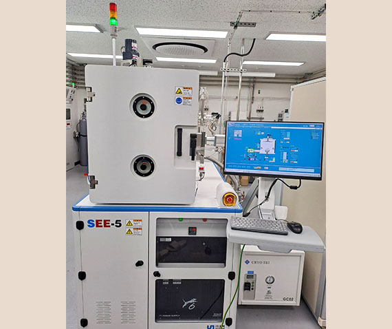
Metal Organic Chemical Vapor Deposition
Location
  • Building 35 (Natural Sciences Hall 5)
Specifications
  • 2000mm×1380mm
Description
  • An instrument that grows solid thin films using metal-organic compounds as precursors.
Applications
  • Used for high-quality thin film fabrication in applications such as LEDs, semiconductor devices, high-frequency components, and power devices.
장비 이미지
No. 12
Sputtering
Location
  • Building 35 (Natural Sciences Hall 5)
Specifications
  • Equipped with Mo, W, and Ni targets.
Description
  • An instrument that uses plasma ions to bombard a target material, causing fine particles to sputter off and deposit as a thin film on a substrate.
Applications
  • Applications include semiconductors, displays, solar cells, and metal thin-film coatings.
장비 이미지
No. 13
Rapid Thermal Processing
Location
  • Building 35 (Natural Sciences Hall 5)
Specifications
  • 1250℃
Description
  • A thermal processing instrument that rapidly heats or cools substrates.
Applications
  • Applications include semiconductor processes such as annealing and dopant activation, thin film crystallization, and junction formation.
장비 이미지
No. 14
Plasma-Chemical Vapor Deposition
Location
  • Building 35 (Natural Sciences Hall 5)
Specifications
  • Capable of using gases such as H2, N2, H2S, and CH4; pressure can be controlled via a throttle valve; plasma generation is possible.
Description
  • A chemical vapor deposition (CVD) system that uses plasma to deposit thin films.
Applications
  • Applications include semiconductor thin film fabrication, displays, solar cells, sensors, and protective coatings.
장비 이미지
No. 15
Graphene-Chemical Vapor Deposition
Location
  • Building 35 (Natural Sciences Hall 5)
Specifications
  • Gases used: H2, N2, CH4
Description
  • An instrument that deposits thin films by using heat to decompose gaseous precursors.
Applications
  • Applications include graphene synthesis, thin film deposition, and thin film fabrication.
장비 이미지
No. 16
Electrochemical Workstation
Location
  • Building 35 (Natural Sciences Hall 5)
Specifications
  • Maximum current: ±5 A, maximum voltage: ±10 V, current accuracy: 0.6 aA, impedance base frequency range: 10 μHz to 8 MHz.
Description
  • An electrochemical analysis instrument capable of performing various experiments such as LSV (Linear Sweep Voltammetry), CV (Cyclic Voltammetry), and EIS (Electrochemical Impedance Spectroscopy).
Applications
  • Electrochemical applications including water-splitting catalyst evaluation, battery research, sensor development, and corrosion studies.
장비 이미지
No. 17
Probe Station
Location
  • Building 35 (Natural Sciences Hall 5)
Specifications
  • Temperature controllable.
Description
  • An instrument that measures the electrical properties of semiconductor devices or materials using microprobes.
Applications
  • Applications include semiconductor device development, material property evaluation, and electrical reliability testing.
장비 이미지
No. 18
Thermal Evaporator
Location
  • Building 35 (Natural Sciences Hall 5)
Specifications
  • Capable of depositing various thin films depending on the deposition source.
Description
  • An instrument that forms thin films on a substrate by vaporizing metals or organic materials using resistive heating.
Applications
  • Applications in thin-film device fabrication, including semiconductor electrodes, optical coatings, OLEDs, and solar cell manufacturing.

[51140] 305, BAC (formerly Dongbaek Hall, Building No. 3) G-LAMP Project Group Changwon National University,
20 Changwondaehak-ro, Uichang-gu, Changwon-si, Gyeongnam, Korea

© Changwon National University. All rights reserved.
G-LAMP NOTICE