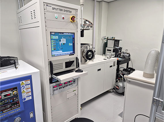
Substrate Module – Susceptor: compatible with 4-inch wafers, deposition thickness non-uniformity below 3%; Rotation Module: variable, controllable from 0 to 50 rpm; Substrate Heating Module: 100–250°C (temperature uniformity within 3%).
Deposition Source – Equipped with two 3-inch targets compatible with RF and DC power; includes one RF power supply (600 W, 13.56 MHz) with shutter; supports multilayer thin film deposition and can mount assist sources during thin film deposition.
Description
A PVD-type functional sputtering system that precisely controls thin film properties, used for depositing oxide or other metal films and producing samples for research and production.
A system that performs magnetron sputtering processes at a vacuum of 10-4 Torr and applies a bias ring to maximize the properties of IGZO and TCO thin films.
Applications
Fabrication of TFT channel layers and sensor thin films.
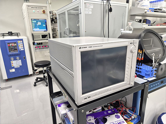
No. 2
Semiconductor inspection equipment
Location
Room 302, Building 55 (Engineering Hall 5)
Specifications
Keysight B1520A
Description
Inspection equipment for semiconductor testing
Applications
Semiconductor testing, sensor measurement, and related applications.
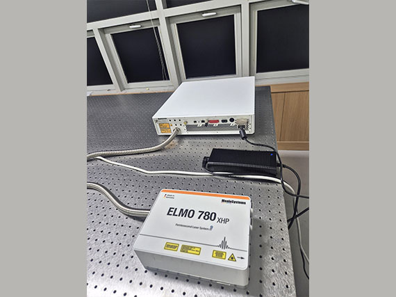
No. 3
Femtosecond laser
Location
Room 302, Building 55 (Engineering Hall 5)
Specifications
ELMO 780 WHP, pulse power 1W>, pulse length<120fs, 780㎚
Description
Laser for multiphoton polymerization 3D printing
Applications
3D printing, laser cutting, and related applications.
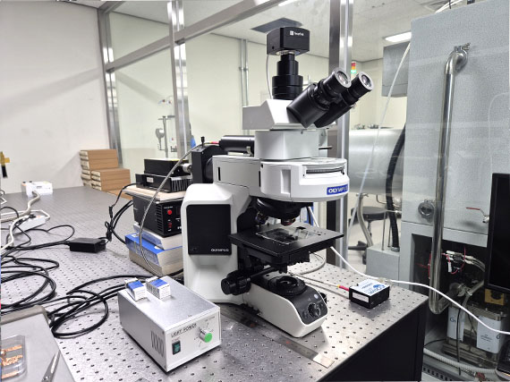
No. 4
Optical microscope
Location
Room 302, Building 55 (Engineering Hall 5)
Specifications
Olympus BX 53
Description
Used for observing displays, cells, and more with high resolution and clear images from UV to near-infrared wavelengths.
Applications
Display quality evaluation, nano/microstructure observation, 3D printing, and related applications.