Advanced Device Desigan Lab. > individual

본문 바로가기
사이트 내 전체검색

Individual Labs

HOME Facilities Individual Labs

Advanced Device Desigan Lab.

Professor

  • Professor Yongsuk Oh

Available Equipment

장비 이미지
No. 1
Laser Patterning System
Location
  • Room 108, Building 50 (Engineering Laboratory 1)
Specifications
  • Dimensions: 950 × 1250 × 1800 mm (x, y, z)
  • Cutting Range: 150x150 (x,y,z)
Description
  • A microfabrication system based on a 532 nm wavelength pulsed laser capable of patterning and cutting.
Applications
  • Used for micro-patterning of ultra-small biomedical sensors and fabrication of microchannels.
  • Capable of precise micro-scale processing on various substrates.
장비 이미지
No. 2
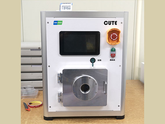
Plasma Surface Treatment System
Location
  • Room 108, Building 50 (Engineering Laboratory 1)
Specifications
  • Dimensions: 440 × 500 × 560 mm (x, y, z)
Description
  • An instrument that uses low-pressure or atmospheric plasma to clean, activate, and coat material surfaces.
Applications
  • Improves molecular bonding efficiency through surface hydrophilicity modification.
  • Enhances detection sensitivity and response speed by activating the gas sensor’s sensing layer.
장비 이미지
No. 3
Workstation
Location
  • Room 108, Building 50 (Engineering Laboratory 1)
Specifications
  • CPU: Intel Core 13th Gen i7-13700K
  • RAM: 128GB DDR4
  • GPU: NVIDIA Geforce RTX 3070
Description
  • Computing equipment for sensor design and data processing equipped with high-performance CPU, GPU, and large-capacity memory.
Applications
  • Performs finite element analysis (FEA) and simulations based on the active layer mechanism inside sensors.
  • Used for real-time sensor data acquisition and high-resolution signal processing.
  • Supports composite sensor network monitoring and integrated system control.
장비 이미지
No. 4
Universal Test Machine
Location
  • Room 108, Building 50 (Engineering Laboratory 1)
Specifications
  • Load Cell Range: 50N Load Cell
Description
  • Performs tensile, compression, and bending tests on various materials to measure mechanical properties.
Applications
  • Evaluation of mechanical strength and reliability of sensor substrates and packages.
  • Performs sensitivity and linearity verification of strain gauges and deformation sensors.
  • Fatigue life and durability testing of wearable and implantable ultra-small biosensors.
장비 이미지
No. 5
Keithley 2450 SourceMeter
Location
  • Room 108, Building 50 (Engineering Laboratory 1)
Specifications
  • Output and range: 20 W, ±200 V / ±1 A, supports four-quadrant sourcing and sinking.
  • Precision and resolution: 6½-digit, 0.012% basic accuracy; voltage resolution 10 nV (20 mV–200 V), current resolution 10 fA (10 nA–1 A).
Description
  • Precision instrumentation capable of accurately sourcing and measuring voltage and current.
Applications
  • Performs I–V characteristic measurements and sensitivity analysis of electrochemical biosensors.
  • Evaluation of low-power operation characteristics and hysteresis of pressure and strain sensors.
  • Precise measurement of current response and photoelectric efficiency of photodetector sensors.
장비 이미지
No. 6
Spin Coater
Location
  • Room 108, Building 50 (Engineering Laboratory 1)
Specifications
  • Dimensions: 260 × 285 × 394 mm (x, y, z)
Description
  • Precision spin coating capable of uniformly applying functional thin films in liquid form.
Applications
  • Controls desired film thickness by precisely adjusting rotation speed and operation time.
  • Enhances microstructure lithography resolution by surface planarization during the thin film coating process.
  • Ensures process reproducibility by maintaining consistent thickness and surface quality with repeated coating under identical speed, time, and liquid viscosity conditions.
장비 이미지
No. 7
Planetary Centrifugal Mixer
Location
  • Room 108, Building 50 (Engineering Laboratory 1)
Specifications
  • Dimensions: 390 × 300 × 340 mm (x, y, z)
Description
  • Mixing equipment that homogenizes samples and performs degassing through centrifugal and orbital motions.
Applications
  • Uniform dispersion of nanoparticle-based sensor precursors.
  • Degassing and homogeneous mixing of enzyme and antibody solutions.
  • Optimization of mixing for composite sensor materials.
장비 이미지
No. 8
Natural Convection Oven
Location
  • Room 108, Building 50 (Engineering Laboratory 1)
Specifications
  • Dimensions: 660x625x810mm(x,y,z)
Description
  • A laboratory thermal oven that uniformly heats and dries samples using natural convection.
Applications
  • Drying of sensor substrates.
  • Sintering and thermal activation of sensing layers.
  • Removal of residual solvents and stabilization of structure.
장비 이미지
No. 9
Fume Hood
Location
  • Room 108, Building 50 (Engineering Laboratory 1)
Specifications
  • Dimensions: 2100x1700x2600mm (x,y,z)
Description
  • Ventilation equipment that safely exhausts hazardous chemical gases and vapors outside the laboratory to protect the environment.
Applications
  • Safe exhaust system for hazardous gases used in gas sensor development.
  • Isolation of contaminants during sensor precursor synthesis processes.
장비 이미지
No. 10
DLP 3D printer
Location
  • Room 108, Building 50 (Engineering Laboratory 1)
Specifications
  • Dimensions: 335x200x300mm (x,y,z)
Description
  • A DLP-type 3D printer capable of fabricating high-resolution microstructures using UV-curable resin.
Applications
  • Microchannel and mold prototyping for microfluidic biosensor chips.
  • Fabrication of waveguides and micro-optical path structures for optical sensors.
  • Custom housing fabrication for wearable biosignal sensor modules.
장비 이미지
No. 11
UV Curing Chamber
Location
  • Room 108, Building 50 (Engineering Laboratory 1)
Specifications
  • Dimensions: 350x350x400mm (x,y,z)
Description
  • A chamber that supports rapid curing of photopolymer resins and coatings using UV LEDs or mercury lamps.
Applications
  • UV curing of optical sensor lenses and waveguide coatings.
  • Photolithography resin curing for microfluidic biosensors.
  • UV curing of electrochemical sensor module joints.
장비 이미지
No. 12
Ultrasonic Cleaner
Location
  • Room 108, Building 50 (Engineering Laboratory 1)
Specifications
  • Dimensions: 390x270x310mm (x,y,z)
Description
  • Cleaning equipment that uses ultrasonic vibrations to finely remove contaminants from sample surfaces.
Applications
  • Removal of residual contaminants within microstructures of MEMS sensor chips.
  • Removal of particulate contamination from optical sensor lenses and prism surfaces.
  • Improvement of experimental reproducibility through cleaning of electrochemical biosensor electrodes.
장비 이미지
No. 13
VHX-7000N
Location
  • Room 108, Building 50 (Engineering Laboratory 1)
Specifications
  • Optical and digital magnification: 1/1.8″ 3.19 MP CMOS sensor (VHX-7020), supports 20× to 500× automatic zoom.
  • Observation and measurement capabilities: supports automatic depth synthesis, 3D profiling, and multiple observation modes including bright-field, dark-field, polarization, and DIC (Differential Interference Contrast).
Description
  • A high-resolution digital microscope system equipped with a 4K CMOS sensor and high-magnification zoom lens.
Applications
  • 3D shape measurement of sensor surfaces and microstructures.
  • Measurement of thin film coating thickness and surface roughness.
  • Quality inspection of sensor module assembly and bonding joints.
장비 이미지
No. 14
Motion Detection Device
Location
  • Room 108, Building 50 (Engineering Laboratory 1)
Specifications
  • Dimensions: 1.3MP/240FPS
Description
  • Motion detection equipment composed of a high-speed, high-sensitivity vision sensor camera and a multi-axis adjustable mount.
Applications
  • Synchronized video acquisition of motion sensors and cameras.
  • Performance verification of gesture recognition algorithms.
  • Evaluation of smart environment motion monitoring systems.
장비 이미지
No. 15
Digital Hotplate Stirrer
Location
  • Room 108, Building 50 (Engineering Laboratory 1)
Specifications
  • Dimensions: 185x185mm (x,y)
Description
  • A digital hotplate stirrer equipped with temperature control and adjustable stirring speed functions.
Applications
  • Sample heating and stirring.
  • Independent control of temperature and stirring speed.
  • Reaction testing and optimization.
장비 이미지
No. 16
Multi Digital Hotplate Stirrer
Location
  • Room 108, Building 50 (Engineering Laboratory 1)
Specifications
  • Dimensions: 500x430x130mm (x,y,z)
Description
  • Heating and stirring equipment capable of simultaneous multi-channel control of multiple digital hotplates and stirring motors.
Applications
  • Simultaneous heating and stirring of multiple samples.
  • Independent temperature and speed control for each channel.
장비 이미지
No. 17
LH-TP50 35L
Location
  • Room 108, Building 50 (Engineering Laboratory 1)
Specifications
  • Capacity and control range: 35 L; temperature: -20 to +150 °C (resolution 0.01 °C, accuracy ±0.3 °C, uniformity ±0.9 °C); humidity: 20 to 95% RH (resolution 0.1% RH, accuracy ±2.0% RH, uniformity ±1.5% RH).
Description
  • A 35 L desktop-type temperature and humidity controlled chamber with temperature and humidity regulation capabilities.
Applications
  • Evaluation of sensor performance characteristics under varying environmental conditions.
  • Thermal and humidity durability testing of biosignal sensors.
  • Stress testing of gas, optical, and electrical sensors.
장비 이미지
No. 18
COOLUV-150
Location
  • MEMS Room, Building 7 (Shared Laboratory and Training Center)
Specifications
  • Dimensions: Light source module, Lamp type : 210W, Wavelength : 350nm to 450nm 이내, Max. beam size : 6in. x 6in., 365nm Intensity : 15 mW/cm2, Beam uniformity : ±3% (4in.) 이하
Description
  • Industrial UV curing equipment equipped with a 6-inch wide UV LED light source and forced air cooling system.
Applications
  • Performs microstructure patterning using photoresist and masks.
  • Enables precise alignment between existing and new patterns using a microscope.
장비 이미지
No. 19
ME-32H Metallurgical microscope
Location
  • MEMS Room, Building 7 (Shared Laboratory and Training Center)
Specifications
  • Dimensions: 260x456x496mm(x,y,z)
  • Magnification: Equipped with 5×, 10×, 20×, 40×, and 60× objective lenses; polarization functionality; equipped with Sony IMX385 CMOS sensor.
Description
  • A system combining a high-resolution optical microscope and a CMOS monitoring camera, enabling fine observation and real-time image acquisition.
Applications
  • Microstructure and defect analysis of MEMS sensor structures, sensor chip surface analysis, and process monitoring.
장비 이미지
No. 20
FT-470Q
Location
  • MEMS Room, Building 7 (Shared Laboratory and Training Center)
Specifications
  • Dimensions: 650x580x1850mm(x,y,z)
Description
  • Temperature-controlled refrigeration equipment capable of stably storing various chemical reagents at a constant temperature.
Applications
  • Maintains temperature stability of PR and developer for MEMS photolithography processes.
  • Stable storage and maintenance of photoresist and developer chemicals.

[51140] 305, BAC (formerly Dongbaek Hall, Building No. 3) G-LAMP Project Group Changwon National University,
20 Changwondaehak-ro, Uichang-gu, Changwon-si, Gyeongnam, Korea

© Changwon National University. All rights reserved.
G-LAMP NOTICE